Powered by P‑Ban: The Japanese Infrastructure Behind PCBFlash
Share
P‑Ban.com is more than just a partner of PCBFlash. It is the core engine powering our North American PCB service. While Mitsui supports logistics and business development, P‑Ban provides the e-commerce infrastructure, manufacturing tools, and partner fab network that make PCBFlash possible.
🚀 What P‑Ban.com Offers
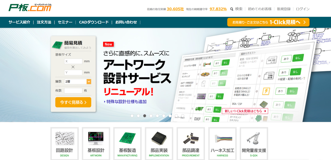
Founded in 2002, P‑Ban.com offers a web‑based platform where users can upload design files, get instant pricing, and order prototypes or small‑volume PCBs with no tooling fees. Over 30,000 engineers—working at renown Japanese companies such as Sony, Toyota, Panasonic & many more—rely on the platform.
🔧 Key Features Engineers Use
- Zero initial tooling fees even for flexible or multilayer boards. P‑Ban prototype tool page
- Next‑day delivery options and a reported 99 percent on‑time shipping rate. P‑Ban main site
- Browser‑based CAD platform with access to 19,000 component footprints and built‑in CAM tools. P‑Ban main site
- Wide board portfolio that includes rigid-flex, high-layer, metal-core, impedance-controlled, and build-up boards. Wikipedia (JP)
- Assembly services for small runs using lead-free solder, BGA/CSP rework, and BOM management. KiCad blog
- Waste board recycling with free collection and reuse discounts. Wikipedia (JP)
🏅 Community Recognition Through GUGEN
P‑Ban is the organizer of GUGEN, one of Japan's largest hardware creation contests. Since 2009, GUGEN has celebrated innovations that solve real‑world problems, with winners receiving cash prizes and PCB/electronic sponsorships. The platform’s involvement in GUGEN demonstrates its commitment to education and community development. GUGEN 2022 press release
🔗 How PCBFlash Leverages P‑Ban
PCBFlash is built on P‑Ban’s capabilities. After reviewing your PCB data, we match it to the best factory within P‑Ban’s fab network or another trusted fab, depending on board type and delivery needs. You see the ease of P‑Ban with added regional options through PCBFlash.
👷 Why This Matters for Engineers
- Fast prototyping without hidden setup costs.
- Access to advanced board types—including HDI, flex, and build-up—without large minimums.
- Assembly with component placement, fine-pitch rework, and BOM integration.
- Secure shipping and logistics support backed by Mitsui’s network.
📌 Final Thoughts
P‑Ban.com is the core platform enabling engineers to access high-quality PCB fabrication in Japan. PCBFlash serves as the gateway for North American customers who want Japanese reliability with global reach. It's not just a partner—it is the engine.
🛠️ Ready to Get Started?
Submit your design through our Custom PCB Order page. Let us connect you to P‑Ban or another fab in its network that fits your needs for speed, quality, and capability.