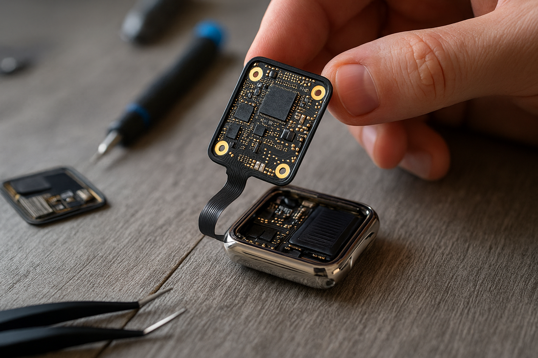
Miniaturization Achieved: Success with 6-Layer Build-Up PCB Prototype
In the development of electronic devices, miniaturization is always a core
element. Especially for wearable devices and communication modules, even a few millimeters difference in PCB size can directly impact product competitiveness.
We developed a successful prototype using a 6-layer build-up PCB to meet a customer’s request for maximum board miniaturization in their new product design.
Our Challenge: Minimizing PCB Size
With conventional multilayer PCBs, there are limits to miniaturization due to wiring space
constraints and design limitations of through-holes.
Therefore, for this design, we adopted:
• A 6-layer structure
• Build-up method (forming fine wiring by stacking)
Build-up PCBs are very effective for high-density mounting and miniaturization because
they allow for laser vias and fine-line wiring. However, creating design data (especially for ArtWork data) requires different rules and know-how compared to standard PCBs.
Our Approach: Support and Standards
The customer approached us with a concern: “We’re not sure how to create AW data.” This was understandable, as the build-up method introduces several design considerations that differ significantly from conventional multilayer PCBs, including:
• Placement rules for laser vias
• How to specify stack-up (layer structure)
• Build-up-specific design constraints (minimum land diameter, line width/spacing)
To support the customer, we provided clear manufacturing standards and hands-on guidance from our expert team. Together, we reviewed their design data and walked through the correct process for creating AW data.
Our Result: Successful Prototype Delivered
Despite it being their first build-up PCB design, the customer successfully prepared manufacturing-ready data, leading to a smooth prototype build. The final 6-layer PCB met miniaturization goals and optimized the mounting area. Positive evaluation results cleared the way for the next stage of product development.
Ready to Shrink Your PCB?
Miniaturization isn’t just about smaller boards—it’s about smarter design. From layer stack-up to via design, every decision influences how compact, efficient, and high-performing your PCB can be.
Upload your files here, and let's build smaller together without compromise!