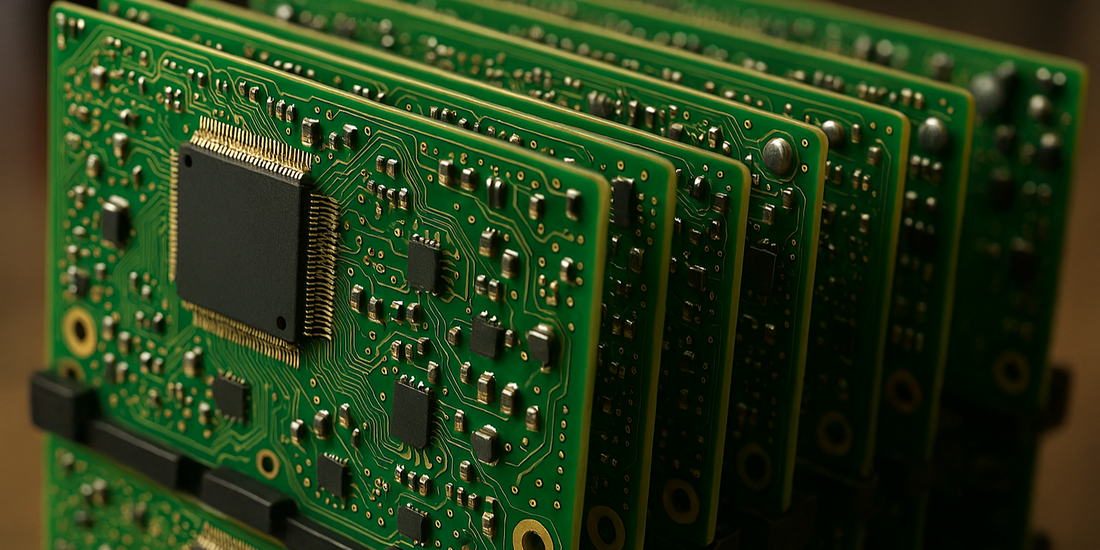
Misaligned Drill Data: Tiny Errors, Major PCB Failures
When designing printed circuit boards, the drilling process is a critical manufacturing step. Through-holes and vias are like the “blood vessels” of a PCB. If their placement is off, the entire board can malfunction. Understanding the causes, effects, and countermeasures for this problem is a vital part of manufacturing.
What is Origin Misalignment?
PCB data is broadly divided into two types:
• Gerber data (wiring and pad information)
• Drill data (hole processing information)
These are overlaid during processing. If their “reference points (origins)” are not aligned,
the hole positions will be off. This misalignment will directly cause PCB defects.
Common Defect Examples
-
Hole Off-Center from Pad
Through-holes are not drilled at the center, causing the land to be missing on one side. This not only affects appearance but also greatly reduces soldering reliability.
-
Via Disconnection
If the via is misaligned in inner layers or micro vias, it might fail conduct entirely. Especially in high-density boards, even a “tens of microns” misalignment can be critical.
-
Interlayer Connection Failure
The inner layer pattern and hole are misaligned, causing open circuit defects. In the worst-case scenario, the entire lot may become defective.
A minor deviation in drill alignment can lead to complete failure, making it a serious concern in PCB manufacturing!
Why Does Misalignment Occur?
- Differences in CAD Specifications: The Excellon format for drill data may define origins slightly differently depending on the tool.
- Reference Point Mix-Up: The designer sets the origin at the “bottom left of the board,” but the manufacturer uses the “center of the board”.
- Mistakes During Panelization or Data Integration: When combining multiple boards, the reference point may remain misaligned.
How to Prevent Misalignment
- Set the Origin During Design: Fix the origin at “bottom left” or “center of the board” in CAD
- Overlay Check During CAM Process: Actually overlaying the drill and Gerber data to confirm alignment.
- Unified and Shared Design Rules: Determine and communicate the origin point to both the design and manufacturing teams.
Quality Assurance Through Data Review
We occasionally receive PCB data from customers where the drill data origin doesn't align with the Gerber data. If manufactured as-is, the through-holes would be off from the pads, and lot defects would have been unavoidable.
At PCB Flash, we always overlay and check the Gerber and drill data after
receiving an order. This workflow allows us to detect abnormalities and request corrections from the customer and prevent manufacturing defects before they occur. Even small setting mistakes can be caught and corrected through data checks before manufacturing, preventing them from turning into major issues.
Ready to Send Us Your Files?
If you’re preparing a custom PCB order, and want to avoid costly mistakes, trust your PCB orders to the industry's most reliable experts!
Upload your files here, and our team will take a close look to ensure everything is in place for a smooth and accurate production run.